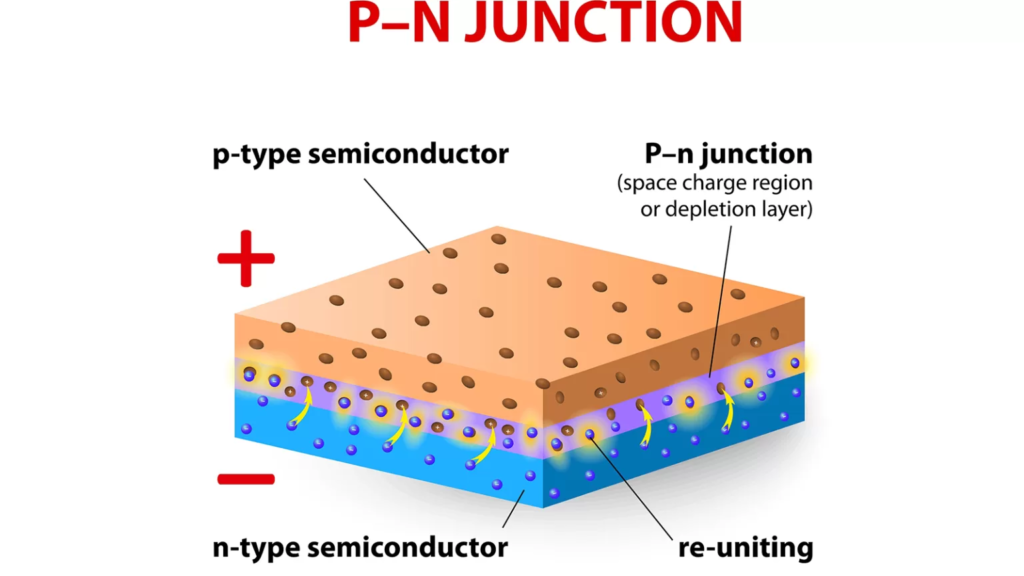
The process of generating power with solar panels is mostly dependent on one essential stage. Electrons go from the valence band (in the solar panel’s PN junction) to the conduction band (in an external circuit, such as a battery). Electrons that are in the valence band and do not have any external energy are referred to as such. To generate electricity, these electrons must travel into the external circuit, also known as the conduction band.
Electrons do not go from the valence to the conduction band on their own. A specific amount of energy (referred to as the band gap) is required to facilitate this shift.
Table of Contents
What is a Band Gap?

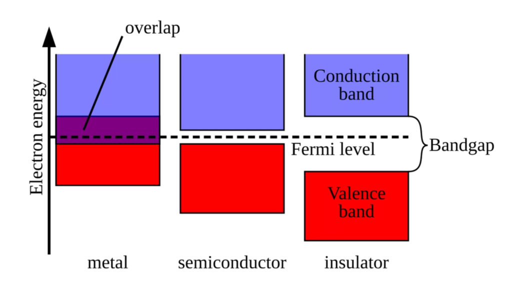
The band gap is an important term in semiconductor materials; it refers to the minimal energy required for electrons to leap to a higher energy level. This is analogous to youngsters requiring sufficient effort to hop to the next square in hopscotch.
Also read: Understanding Different Types of Solar Panels
The size of the band gap controls the range of photon wavelengths that a material can absorb, which is critical for generating current in solar panels by efficiently absorbing photons from the entire solar spectrum. Varying band gap sizes allow materials to optimize photon absorption in high or low-energy light regions, adjusting to a wide range of environmental and application requirements.

In conductors, there is no gap between the conduction and valence bands, hence the conduction band is filled with electrons, creating the substance. Because there is no gap between the conduction and valence bands in conductors, the conduction band is filled with electrons, resulting in a highly conductive material.
Insulators, on the other hand, have a huge gap between the valence and conduction bands, preventing electrons in the valence band from jumping to the conduction band and therefore rendering the material non-conductive. Semiconductors typically have a band gap that falls between these two extremes, making them non-conductive. When energy is added (by light, heat, etc.), electrons in the valence band can migrate into the conduction band, allowing the material to conduct electricity.
Why is the Band Gap Important?
Solar cells work by absorbing energy from sunlight, causing electrons to jump to higher energy levels and generate an electric current. The band gap controls which energy particles (photons) in sunlight the solar cell can absorb. If the band gap is too high, many photons lack the energy to cause electrons to jump.
If the band gap is too tiny, extra energy will be lost. As a result, the proper band gap enables solar cells to convert sunlight into electricity more efficiently
Why Is The Band Gap of 1.5 eV Considered Optimum?

The band gap of 1.5 eV is considered optimum for solar cell efficiency for a few key reasons:
Matching the Solar Spectrum
A band gap of around 1.5 eV allows the solar cell to absorb a significant portion of the solar spectrum, particularly in the visible light range. This is because the energy of photons in the visible spectrum corresponds well to a band gap of 1.5 eV. Photons with energies greater than 1.5 eV can excite electrons across the band gap, generating electron-hole pairs that can be collected as current.
Limiting Efficiency Considerations
The Shockley-Queisser limit, which calculates the maximum theoretical efficiency of a single-junction solar cell, shows two peaks. The larger peak occurs at a band gap of 1.34 eV with a limiting efficiency of 33.7%. The smaller peak is around 1.1 eV with an efficiency limit of nearly 32%. Silicon, with a band gap of 1.11 eV, is close to this smaller peak. However, a band gap of 1.5 eV is closer to the absolute maximum and provides a good balance between absorption and voltage.
Practical Considerations
While the theoretical limit for a 1.5 eV band gap is slightly lower than the 1.34 eV peak, 1.5 eV is a more practical choice. Materials with a 1.5 eV band gap, such as gallium arsenide phosphide (GaAsP) and perovskites, can be more easily fabricated into high-quality solar cells. Silicon, while abundant and inexpensive, has some limitations due to its indirect band gap. A 1.5 eV direct band gap material can absorb light more strongly and generate electron-hole pairs more efficiently.
Multijunction Optimization
When used in multijunction solar cells, a 1.5 eV band gap material can serve as an excellent top cell. By combining it with lower band gap materials like germanium (0.67 eV) or silicon (1.11 eV) in a tandem configuration, the overall efficiency can be significantly boosted. The 1.5 eV top cell absorbs the high-energy photons while allowing the lower-energy photons to pass through to the bottom cell, enabling more complete utilization of the solar spectrum.
Book Best Solar Panel on No Cost EMI
Also read: What are the Main Components of Solar Panel?
Band Gap Values of Different Materials
Conductors
- Metals: Generally, metals do not have a band gap, as their valence and conduction bands overlap, allowing electrons to move freely. This results in high electrical conductivity.
Semiconductors
- Silicon (Si): Band gap of approximately 1.1 eV. Silicon is the most widely used semiconductor in electronics and solar cells due to its suitable band gap for absorbing visible light.
- Gallium Arsenide (GaAs): Band gap of about 1.42 eV. GaAs is used in high-efficiency solar cells and optoelectronic devices due to its direct band gap, which allows for efficient light absorption and emission.
- Indium Phosphide (InP): Band gap of around 1.34 eV. InP is used in high-frequency and high-power applications, including fiber optic communications.
- Cadmium Telluride (CdTe): Band gap of approximately 1.5 eV. CdTe is commonly used in thin-film solar cells, making it a significant material in photovoltaic technology.
- Gallium Nitride (GaN): Band gap of about 3.4 eV. GaN is utilized in high-power and high-frequency applications, including LEDs and power transistors.
Insulators
- Diamond: Band gap of around 5.5 eV. Diamond is an excellent electrical insulator and has high thermal conductivity, making it useful in various applications.
- Aluminum Oxide (Al2O3): Band gap of approximately 8.8 eV. This material is widely used as an insulator in electronic devices.
- Silicon Dioxide (SiO2): Band gap of about 8.9 eV. SiO2 is commonly used as an insulator in semiconductor devices and as a dielectric material.

Importance of Band Gap in Applications
The band gap influences the electrical conductivity and optical properties of materials, making it a critical factor in the design of electronic and optoelectronic devices. For example:
- Solar Cells: The ideal band gap for solar cells is around 1.1 to 1.5 eV, as this range allows for optimal absorption of sunlight while maximizing the conversion of solar energy into electricity.
- LEDs: The band gap determines the color of light emitted by LEDs. Materials with smaller band gaps emit longer wavelengths (red), while those with larger band gaps emit shorter wavelengths (blue).
- Transistors: The choice of semiconductor material and its band gap are essential for the performance of transistors in electronic circuits, affecting switching speeds and power efficiency.


